Professor Chen Rong and other researchers in her group have identified several critical issues in the field
“Atomic deposition is a universal technologyfuture-oriented deposition, which will play an increasingly important role in the field of micro-nanofabrication. Chip manufacturers have shown great interest in this technology. In addition to the field of microelectronics, atomic scale deposition has a wide range of applications in optoelectronics, energy storage, catalysis, and biomedicine,” says Professor Rong.
 Downscaling of nanomaterials, nanostructures, nanodevices and nanosystems requires the application of atomic-level deposition technology
But to achieve nanomanufacturing with highThe accuracy of the deposition mechanism at the atomic level requires deep study. While characterization technologies are on the rise, the technology for characterizing and manipulating individual atoms still has enormous room for improvement. Complex nanostructures require a combination of several processes for different materials. However, in order to achieve process integration, it is necessary to take into account the accuracy and efficiency of processing as mutually inhibiting factors.
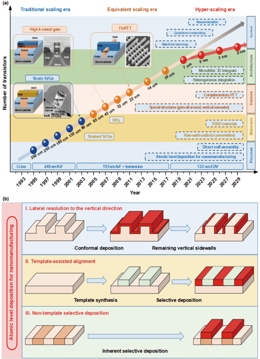
The researchers hypothesized that the deposition onatomic level can be used to extend Moore's law. Atomic-level deposition is an increasingly promising technology for the precise fabrication of complex nanostructures, enabling the creation of equivalent topography with better control of film thickness and without surface roughness. It is considered the cutting edge technology for the production of semiconductor assemblies.
Recall that after the industry has successfullydeveloped strained Si/Ge, high-potassium/metal gate and fin FETs, the critical size of FETs has been reduced to 7 nm, meaning there are nearly 7 billion transistors per square centimeter on a single chip. This poses enormous challenges for rib structure and nanofabrication methods. So far, extreme ultraviolet lithography has been used in some critical stages, but it faces alignment inaccuracy and high costs in high-volume production.
Back in 1959, Professor Feynman suggested:"There's plenty of room at the bottom." This performance inspired people to manipulate atoms or molecules as building blocks for engineered structures. The first step is sputtering, which provides lateral angstrom resolution in the vertical direction, as well as top-down etching, such as double painting. Various selective template deposition techniques are then used to align complex 3D structures, including dielectric templates, inhibitors, and correction steps. Finally, atomic scale resolution can be achieved through inherently selective deposition.
Deposition methods at the atomic levelare characterized by conformality and homogeneity of thin films. Atomic-level deposition can result in horizontal resolution in the vertical direction for a variety of high aspect ratio structures, including sidewalls, nanowires, nanotubes. The self-aligning double pattern is a typical example of vertical resolution. Deposition at the atomic level can improve the accuracy of the nanostructure and produce some special structures that can further reduce the size of the element and increase the density of transistors, thus contributing to the operation of Moore's law in the short term.
As devices become morecomplex, directed growth of thin films is considered an important aspect of nanomanufacturing. Selective deposition is an effective leveling technique that can shorten steps such as photolithography and etching. Efficient, highly selective deposition is usually achieved by using special templates. With these, chip makers can not only stack transistors directly in three dimensions, but also integrate multi-functional features such as sensors and energy storage into chips to produce superchips.
Prepare suitable templates for selectiveDeposition of low-dimensional materials and complex 3D structures using current top-down approaches is quite difficult. For the post-silicon era, atomic-level deposition is becoming a popular way to create many alternative nanomaterials such as 2D, carbon, ferroelectric, and phase change materials.
Read more:
The James Webb telescope took the first picture of Jupiter: it shows 9 moving targets at once
Scientists understand why T-Rex and other large dinosaurs had small "hands"
The oldest Voyager 1 mission has a strange glitch that cannot be fixed