From “simple” home appliances and computers to solar cells, field-effect transistors and drones
The clear leader in the industry right now is silicon.But it is not suitable for all devices; in addition, the physical properties of the semiconductor limit the possibilities for further miniaturization and increasing the power of chips and the creation of flexible devices. Fortunately, there are other alternative materials.
We tell you how semiconductors work and whatthere are promising alternatives to silicon for the creation of microelectronics. You can read more about the market in general in the July issue of the digest on robotics “Microelectronics. The less, the better”, prepared by Innopolis University.
What is a semiconductor
A semiconductor is a material that, according to its specificconductivity is intermediate between conductors and dielectrics. Typically, it is a crystalline solid. It conducts electricity under certain conditions, making it ideal for controlling the flow of current.
Semiconductors in their normal state conductlittle or no current blocking it. But with an increase in temperature or under the influence of light, they begin to better transmit electric charges. Also, the conductivity of semiconductors changes when an impurity is introduced - this process is called doping.
Important difference between a semiconductor and a conductorlies in the fact that the current in it is carried not only by electrons, but also by the vacancies left by them - holes. Holes remaining in the valence band can be occupied by electrons from lower energy states and thereby contribute to the flow of current.
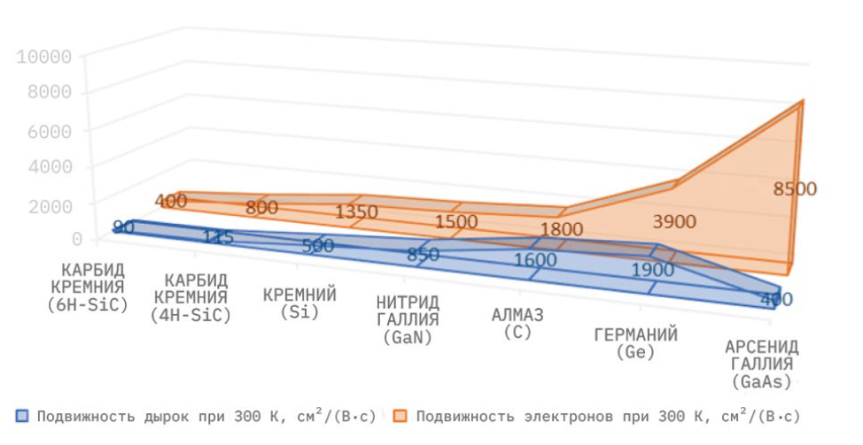
One of the key characteristics of a semiconductor isis the mobility of charge carriers (electrons and holes). This is a coefficient that shows the relationship between the average particle velocity and the applied external electric field. The mobility of electrons and holes can be different, for example, in silicon at room temperature, negatively charged particles move almost three times faster than positive ones.
In addition, semiconductors vary in widthforbidden zone. This is the minimum energy required to move an electron from the valence band to the conduction band. For metals and other semiconductors, it is equal to 0, and when a level of 4 eV or more is reached, the material becomes a dielectric.
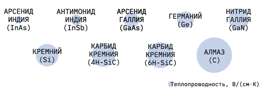
Another important characteristic of semiconductors is thermal conductivity. It shows how quickly and easily it will be possible to remove heat from the components in order to protect the device from overheating.
Silicon
Silicon is second only to carbon in terms ofabundance of a chemical element on Earth. Its main advantage is that it is easy to mine, silicon crystals are relatively easy to work with, and provide good overall electrical and mechanical properties. Even despite the relatively low mobility of electrons and holes, it remains the optimal material for microelectronic production.
Another advantage is that whenwhen used in integrated circuits, it forms high quality silicon oxide, which acts as an insulating layer between various active elements.
To increase the density of elements andspeed of integrated circuits, combinations of elements of single-crystal and polycrystalline silicon are used. And to increase the conductivity of polycrystalline silicon, it is doped.
Silicon semiconductors are widely used forcreation of integrated circuits, bipolar and field-effect transistors, charge-coupled devices, high-speed photodiodes and many other devices. And silicon-based products, such as super-junction MOSFETs or IGBTs, can be used in a wide range of voltages (from a few to several hundred volts) and in various power classes.
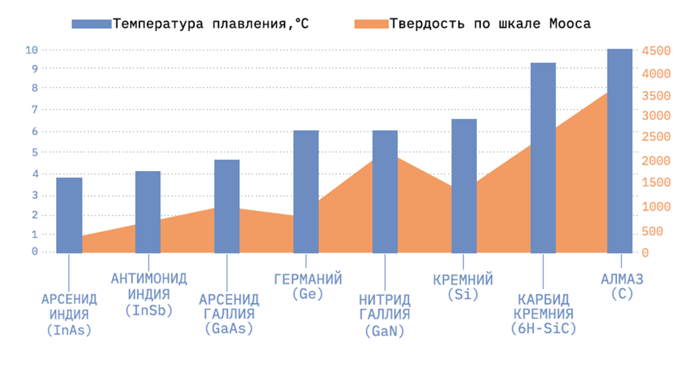
Germanium
We live in the “silicon” era, and maybeIt may seem that microelectronics began with this material, but germanium was the first. It was used in many early devices, from radar detection diodes to the first transistors. Until the end of the 1960s, it was the main semiconductor used in electronic devices, and only in the early 70s was it replaced by silicon.
The new "champion" is much more common, itIt is cheaper to produce and has a wider bandgap and better thermal conductivity. But germanium also has its advantage: the charge carriers in this material are much more mobile.
For example, at a temperature of 300 K (about 27°C), the electrons in the “first” semiconductor move almost three times faster than those of silicon, and the holes move almost four times faster.
Although germanium is not suitable for modernmicroelectronics, due to these properties it is still used in some radio frequency devices. For example, it is used to create microwave devices, audio equipment, as well as low-power and precision equipment.
gallium arsenide
Gallium arsenide is the second mostcommon semiconductor in use today. Unlike silicon and germanium, gallium arsenide is a compound, not an element, and is obtained by combining trivalent gallium with arsenic, which has five valence electrons.
Large bandgap and highThe electron mobility causes gallium arsenide devices to respond quickly to electrical signals, making this compound suitable for amplifying high frequency signals. In addition, this material has shown its efficiency at high temperatures and good resistance to radiation.
Gallium arsenide has long been used inmicroelectronics, so the production of devices based on it is debugged. Due to its special properties, the material is mainly used to create microwave microelectronic devices: digital and analog integrated circuits, discrete field-effect transistors and Gunn diodes, which operate without a p-n junction at the expense of the material's own resources. In addition, gallium arsenide-based microcircuits are used in the manufacture of mobile phones, microwave devices, satellite communication devices and some radar systems.
However, it is a brittle material with lesshole mobility than silicon, which makes it impossible to create devices such as, for example, CMOS transistors, high-speed and energy-saving electronic circuits. It is also relatively difficult to manufacture, adding to the cost of gallium arsenide devices. And it has a fairly low thermal conductivity, which increases the risk of overheating devices.
Materials of the future
— Diamonds
Diamond has a band gap greater than 3 eV, so by definition it is a dielectric. However, when impurities are added, the gemstone becomes a semiconductor.
Theoretically diamond semiconductorThe devices have excellent physical properties, including high thermal conductivity, breakdown field strength, and carrier mobility. This will significantly reduce losses, quickly dissipate heat and increase the service life of devices. In addition, it can operate at an output power and energy efficiency 50,000 times higher than silicon devices and 1,200 times higher frequency.
However, for industrial applications in electronicSemiconductor devices require high-quality, large-sized diamond wafers. Although attempts to create diamond tools have been going on for many years. So far, the problems associated with alloying and processing of the material have not been solved.
— Graphene
Graphene is a two-dimensional allotropic modificationcarbon. Graphene has the potential to surpass silicon as a versatile semiconductor material, McKinsey predicts, but it could take up to 25 years before widespread commercialization.
The key feature of this material is flexibility,therefore, various complex devices can be produced from it. This material is considered promising for its further use, and there are entire institutes around the world dedicated to research and development in the field of graphene.
It can be useful in a variety of industries:from modern energy networks and alternative energy to biomedicine. In microelectronics, graphene can be used in ultrasensitive microprocessors, elements of quantum computers, and sensors with extreme parameters.
— Boron arsenide
As recently as July 2022, researchersfrom MIT said they had found the best semiconductor known. It turned out to be cubic boron arsenide. This material is a compound of arsenic and boron.
Its thermal conductivity is 10 times greater than that ofsilicon Moreover, unlike the latter and gallium arsenide, the boron-based semiconductor demonstrates high mobility not only for electrons, but also for holes.
Although scientists say that this materialpotentially able to replace silicon, but, as with graphene, this is still very far away. For example, first you need to develop cheap ways to produce this material with high quality.
Despite the high popularity and effectivenesssilicon semiconductors, analogues are needed. Manufacturers are being pushed towards this by two factors at once. First, technology has almost reached a limit beyond which it will be impossible to create ever smaller and more powerful devices. And secondly, the constant increase in demand for silicon leads to its rise in price.
The production crisis that arose during the pandemiccoronavirus has shown how dangerous it is to rely on a single source. Therefore, companies and scientists around the world are working to create an alternative. Nevertheless, it can be assumed that, due to the cheapness, availability, and well-established production of silicon devices, this material will hold a leading position in microelectronics for some time to come.
Read more:
“This is science fiction”: scientists create a fundamentally new type of quantum computers
What are supergenes and how do they make animals so weird
The ISS "shoots" laser beams at the Earth: why is it needed and how does it work