Engineers have built a dielectric nanoresonator that concentrates light into a volume that is 12 times
What is the diffraction limit?
Until recently, among physicists there wereIt is widely believed that it is impossible to compress light below the so-called diffraction limit. This is the minimum spot size that can be obtained by focusing electromagnetic radiation.
The exception is the use of metalnanoparticles, which, however, also absorb light. Therefore, it seemed impossible to compress it strongly in dielectric materials such as silicon. And this is a key material for the development of future devices. They have one important advantage - they do not absorb light.
Interestingly, in 2006, scientists theoreticallyproved that the diffraction limit does not apply to dielectrics. However, no one has been able to demonstrate this in practice. The reason is simple - engineers were unable to build the necessary dielectric nanostructure.
Now the employees of the Technical UniversityDenmark succeeded, they built a dielectric nanoresonator that concentrates light in a volume 12 times less than the diffraction limit.
What helped scientists?
Diffraction limit theory describes that lightimpossible to focus in a volume smaller than half the wavelength in the optical system. For example, this affects resolution in microscopes. However, nanostructures can be composed of elements much smaller than the wavelength. This means that the diffraction limit is no longer something fundamental.
When light is compressed, it becomes more intense, enhancing the interaction between light and materials. Particularly dielectric.
What are dielectric materials?
Dielectrics are materials that do not conductelectric current. Glass, rubber and plastic are examples of dielectric materials and contrast with metals, which are electrically conductive. An example of a dielectric material is silicon, which is often used in electronics as well as photonics.
What is the problem?
Although computer calculations show that it is possible to concentrate light into an infinitesimal point, this is only applicable in theory.
In the new study, scientists usedall available knowledge about real photonic nanotechnology and its current limitations and loaded it into a computer. They then “asked” him to find a pattern that collects photons in an unprecedentedly small region—an optical nanocavity. That helped. The device was built in a laboratory at the same university.
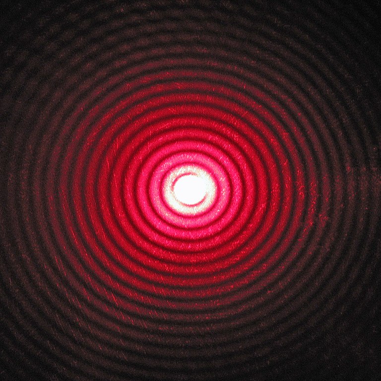 Diffraction pattern of a red laser beam,made on a plate after passing through a small round hole in another plate. Physical optics is used to explain effects such as diffraction. Author: Wisky
Optical nanocavities are structuresspecially designed to hold light, preventing it from spreading. It's like he's trapped between two mirrors, being thrown back and forth. The closer the mirrors are placed to each other, the more intense the light between them becomes.
What is the nanoresonator made of and how?
For a new experiment, physicists have developed a structure in the form of a butterfly. Thanks to its special shape, it compresses photons particularly effectively. The nanoresonator itself was made of silicon.
The material for the nanoresonator was developed in purepremises of the university, and the templates on which the cavity is based were optimized and designed using a unique topology optimization method.
A clean room is a room where the airthe size and number per cubic meter of particles such as dust, microorganisms, aerosol particles and chemical vapors are maintained within a certain predetermined range. There are special international standards for such premises, their cleanliness is ensured by special equipment.
Originally developed for the design of bridges and aircraft wings, the optimization method has been used for nanophotonic structures.
Why is it important?
The authors of the development are confident that their discovery hascritical to developing revolutionary technologies that reduce the number of energy-consuming components in data centers, computers, phones and more.
Energy consumption of computers and centersData processing continues to grow, and there is a need for more resilient chip architectures that consume less power. This can be achieved by replacing electrical circuits with optical components. Scientists hope that a “division of labor” between light and electrons will help here. Everything is like in the Internet, where light is used for communication, and electronics are used for data processing. The only difference is that both functions must be built into the same chip. This is why it is so important to compress light to the same size as electronic components. An experiment by scientists showed that this is indeed possible.
This is an important step towards developing moreenergy-efficient technology, such as nanolasers for optical connections in data centers and future computers. However, engineers still have a long way to go.
What's next?
Scientists plan to continue workingand improve methods and materials to find the optimal solution. They are confident that they will be able to create increasingly intense photons as technology advances. The authors of the development are convinced that this is only the first of a series of major developments in the field of physics and photonic nanotechnology focused on this principle.
Read more:
Archaeologists have officially confirmed the legends from the Bible
It turned out what happens to the cells of the body when the heart dies
Starlink signal hacked to be used as an alternative to GPS